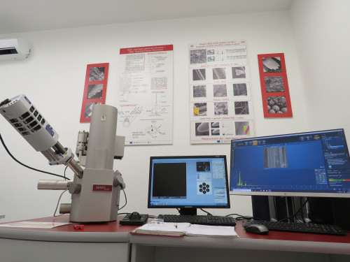
Scanning Electron Microscope with EDS detector
Manufacturer and type
Tescan, Czech Republic, FE-SEM, Mira II LMU;
Location
Department of Textile Chemistry and Ecology
Contact person:
Prof. Sandra Bischof, PhD
sbischof@ttf.unizg.hr
Application:
A scanning microscope with an FE (field emission) electron source enables high-resolution image of the object. It is equipped with several detectors: secondary electron detector (SE), backscattered electron detector (BSE), detector for higher resolution of very short working distances (In-beam SE), X-ray detector for elemental analysis (EDS), detector for the analysis of electric currents in semiconductors, e.g. integrated circuits, solar cells, etc. (EBIC), and a detector which acquires TEM comparable images by using a SEM microscope (STEM). The microscope can operate in low vacuum conditions thus preventing the surface electrostatic charge of the sample. It has a wide range of applications in technical and natural sciences with regard to application in topography and morphology analysis of sample surfaces, particle size distribution, determination of sample dimensions and homogeneity, mechanical and chemical damage to materials and their chemical composition.
Technical characteristics:
- Resolution: 1.0-3.0 nm
- Magnification: 4 x-1.000.000 x
- Electron gun: High brightness Schottky emitter
- Scanning features: Dynamic focus, Point and Line scan, 3D Beam
More from category
- Vacuum system for sample impregnation with resin
- Polishing machine
- Vacuum oven
- Gas Pycnometer
- Vacuum Lab Press
- Laser Cutting Machine
- Critical Point Dryer
- Rotawash Color Fastness Tester
- Apparatus for wet finishing and dyeing - Datacolor
- Apparatus for wet finishing and dyeing - Mathis
- Autoclave for dyeing and finishing
- Automatic Titration Unit
- DSC - Differential Scanning Calorimeter
- Prespotting device
- Digital Textile Inkjet Printing Machine
- TENSOLAB Strength Tester
- Džiger
- EDS Detector
- Electro Kinetic Analyser EKA
- Electrokinetic Analyser SurPASS
- Fourier Transform Infrared Spectrophotometer with TG-IR Interface (TG-IR)
- Fixotest
- Fluorometer HITACHI F-7000 FL
- Fular
- HPLC - Liquid chromatography device
- Analytical scale KERN ALJ 220-5DNM
- Linitest - apparatus for wet finishing and dyeing
- MCC – Microscale combustion calorimeter
- Microtome for precision cutting of samples for electron microscopy
- Sample sputter coater for electron microscopy
- Washing machine
- Pad-Dry-Cure System
- Remission spectrophotometer
- SPECORD 50 PLUS BU
- STEM Detector
- Scanning Electron Microscope with EDS detector
- Spectrophotometer Datacolor 850
- Constant climate chamber
- Sušionik
- Thermogravimetric Analyser (TGA)
- UV-Visible Spectrophotometer UV-2600
- UV/VIS spectrophotometer
- Rotary Drum DIN Abrasion tester
- Device for testing textile dust generation
- FRICTORQ, Fabric Friction Tester
- IULTCS & Veslic Leather Abrasion Tester
- Moisture Management Tester
- Bundesmann water repellency tester
- Limiting Oxygen Index Chamber
- Fabric Touch Tester, FFT
- Coater
- Viskozimetar
- Xenotest 440